Features
- Fully integrated VCO
- Supporting GSM 1800 and GSM 900 standards
- 130nm CMOS technology
- Phase noise of -148 dBc/Hz at 1.8 MHz offset frequency
- LC-tuned Colpitts architecture
- No switching capacitors required
- 3.3 V Design
General Description
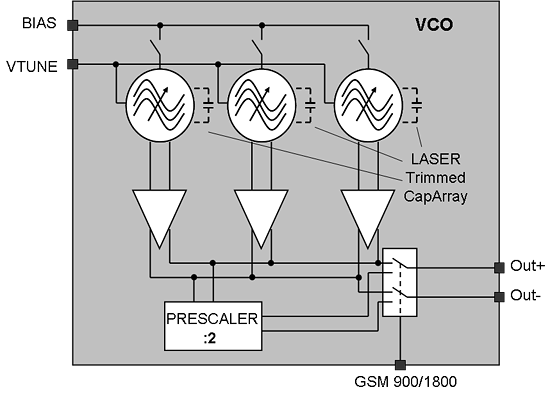
IMST’s base station VCO has been developed for a GSM base station PLL. The GSM 1800 as well as GSM 900 standards can be covered on one die together with the PLL. The architecture comprises three LC-tuned Colpitts oscillators with buffer stages which are alternating be used to cover the required bandwidth. GSM 900 can be used by a selectable frequency divider. Therefore coarse tuning is realized by alternating the selectable VCO circuit in combination with the prescaler and varactor diodes are used for fine tuning.
Block diagram
within the frequency range of each VCO core. In terms of achieving a low phase noise performance, a switchable LC tank is avoided because of the lossy switches. A 130 nm RF-CMOS process was used for the implementation. The process supports thick oxide devices for higher breakdown voltages. Trimming of the three oscillators is done in a post-production process by laser trim option.
| Parameter | Value | Unit | Note |
| VDD | 3,3 | V | |
| IDD | <100 | mA | |
| Frequency range VCO1 | 1500-1670 | MHz | |
| Frequency range VCO2 | 1650-1830 | MHz | |
| Frequency range VCO3 | 1810-1990 | MHz | |
| Phase noise | - 131 | dBc/Hz | At 400 kHz |
| - 137 | dBc/Hz | At 600 kHz | |
| - 148 | dBc/Hz | At 1800 kHz | |
| - 156 | dBc/Hz | 6000 kHz |


